- 您现在的位置:买卖IC网 > Sheet目录3873 > PIC16F627-04/P (Microchip Technology)IC MCU FLASH 1KX14 COMP 18DIP
PIC16F62X
DS40300C-page 154
Preliminary
2003 Microchip Technology Inc.
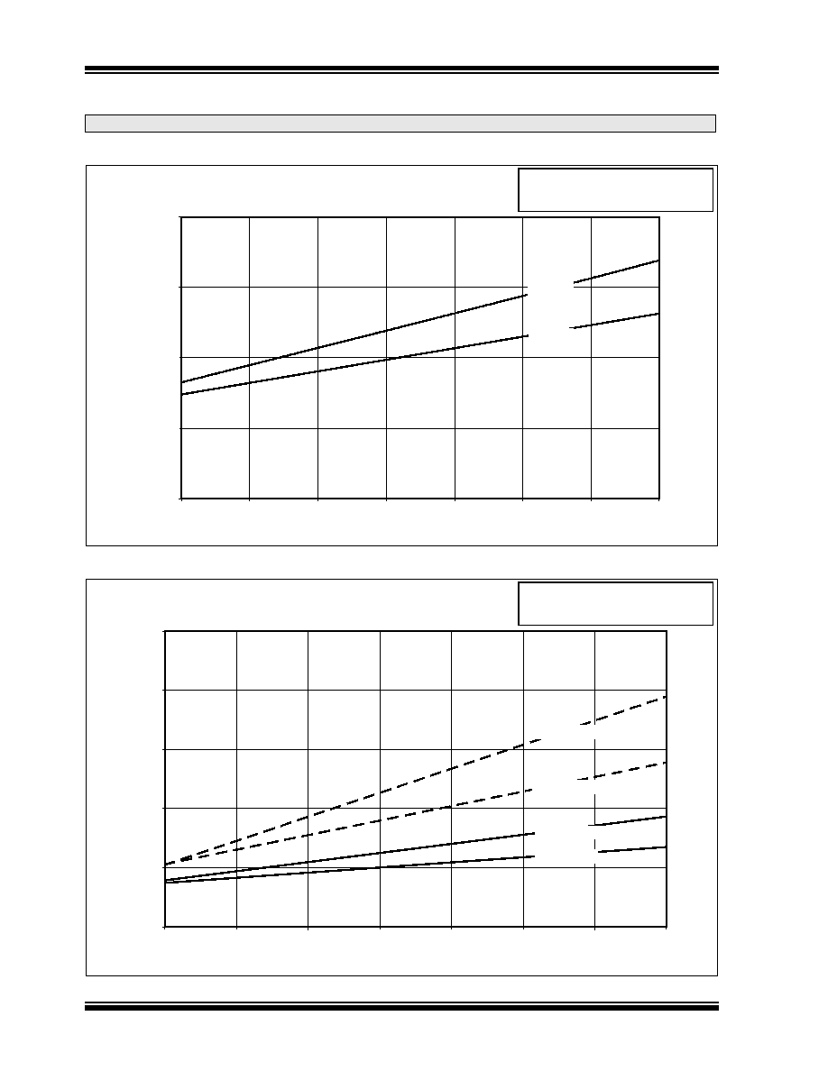
FIGURE 18-22:
VIN VS VDD TTL
FIGURE 18-23:
VIN VS VDD ST INPUT
Note:
The graphs and tables provided in this section are for design guidance and are not tested.
VIN vs VDD
TTL Input
0.0
0.5
1.0
1.5
2.0
2.5
3.0
3.5
4.0
4.5
5.0
5.5
VDD (V)
Vin
(V)
Max (-40C)
Min (125C)
Typical:
statistical mean @ 25°C
Maximum: mean + 3σ (-40°C to 125°C)
Minimum: mean – 3σ (-40°C to 125°C)
VIN vs VDD
ST Input
0.0
1.0
2.0
3.0
4.0
5.0
2.0
2.5
3.0
3.5
4.0
4.5
5.0
5.5
VDD (V)
Vin
(V)
Max High (125C)
Max Low (125C)
Min Low (-40C)
Min High (-40C)
Typical:
statistical mean @ 25°C
Maximum: mean + 3σ (-40°C to 125°C)
Minimum: mean – 3σ (-40°C to 125°C)
发布紧急采购,3分钟左右您将得到回复。
相关PDF资料
PIC18F45J10-I/ML
IC PIC MCU FLASH 16KX16 44QFN
PIC18F24K22-I/ML
IC PIC MCU 16KB FLASH 28QFN
PIC16CR76-I/SS
IC PIC MCU 8KX14 28SSOP
PIC16F887-I/P
IC PIC MCU FLASH 8KX14 40DIP
PIC16CR76-I/SP
IC PIC MCU 8KX14 28DIP
PIC16CR76-I/SO
IC PIC MCU 8KX14 28SOIC
PIC16CR76-I/ML
IC PIC MCU 8KX14 28QFN
PIC16CR74T-I/ML
IC PIC MCU 4KX14 44QFN
相关代理商/技术参数
PIC16F627-04/P
制造商:Microchip Technology Inc 功能描述:IC 8BIT FLASH MCU 16F627 DIP18
PIC16F627-04/SO
功能描述:8位微控制器 -MCU 1.75KB 224 RAM 16I/O 4MHz SOIC18 RoHS:否 制造商:Silicon Labs 核心:8051 处理器系列:C8051F39x 数据总线宽度:8 bit 最大时钟频率:50 MHz 程序存储器大小:16 KB 数据 RAM 大小:1 KB 片上 ADC:Yes 工作电源电压:1.8 V to 3.6 V 工作温度范围:- 40 C to + 105 C 封装 / 箱体:QFN-20 安装风格:SMD/SMT
PIC16F627-04/SO
制造商:Microchip Technology Inc 功能描述:8BIT FLASH MCU SMD 16F627 SOIC18
PIC16F627-04/SO
制造商:Microchip Technology Inc 功能描述:Microcontroller IC Number of I/Os:16
PIC16F627-04/SS
功能描述:8位微控制器 -MCU 1.75KB 224 RAM 16I/O 4MHz SSOP20 RoHS:否 制造商:Silicon Labs 核心:8051 处理器系列:C8051F39x 数据总线宽度:8 bit 最大时钟频率:50 MHz 程序存储器大小:16 KB 数据 RAM 大小:1 KB 片上 ADC:Yes 工作电源电压:1.8 V to 3.6 V 工作温度范围:- 40 C to + 105 C 封装 / 箱体:QFN-20 安装风格:SMD/SMT
PIC16F627-04E/P
功能描述:8位微控制器 -MCU 1.75KB 224 RAM 16I/O RoHS:否 制造商:Silicon Labs 核心:8051 处理器系列:C8051F39x 数据总线宽度:8 bit 最大时钟频率:50 MHz 程序存储器大小:16 KB 数据 RAM 大小:1 KB 片上 ADC:Yes 工作电源电压:1.8 V to 3.6 V 工作温度范围:- 40 C to + 105 C 封装 / 箱体:QFN-20 安装风格:SMD/SMT
PIC16F627-04E/SO
功能描述:8位微控制器 -MCU 1.75KB 224 RAM 16I/O 4MHz Ext Temp SOIC18 RoHS:否 制造商:Silicon Labs 核心:8051 处理器系列:C8051F39x 数据总线宽度:8 bit 最大时钟频率:50 MHz 程序存储器大小:16 KB 数据 RAM 大小:1 KB 片上 ADC:Yes 工作电源电压:1.8 V to 3.6 V 工作温度范围:- 40 C to + 105 C 封装 / 箱体:QFN-20 安装风格:SMD/SMT
PIC16F627-04E/SS
功能描述:8位微控制器 -MCU 1.75KB 224 RAM 16I/O 4MHz Ext Temp SSOP20 RoHS:否 制造商:Silicon Labs 核心:8051 处理器系列:C8051F39x 数据总线宽度:8 bit 最大时钟频率:50 MHz 程序存储器大小:16 KB 数据 RAM 大小:1 KB 片上 ADC:Yes 工作电源电压:1.8 V to 3.6 V 工作温度范围:- 40 C to + 105 C 封装 / 箱体:QFN-20 安装风格:SMD/SMT